Share
+86-021-3700 9238

Products

Home > Products
A series of summaries

Laser solder (Laser Soldering) has the following terms: laser reflux welding (Laser Reflow Soldering), laser tin bond welding (Laser Solder Bonding), laser ball planting (Laser Solder Bumping) but the principle of basic connection is the same. The connection is realized by heating the connection part with laser and melting the solder.

 As a rapid development of laser tin welding technology in recent years, compared with the traditional electric soldering iron technology, laser welding technology is more advanced, heating principle is also different from the former, it is not simply to replace the heating part of the soldering iron. Laser is "surface exothermic", heating speed is very fast, while soldering iron is heating slowly by "heat transfer".

Laser tin welding process

1, laser irradiation to the welding site, to achieve solder melting temperature

2, supply tin solder, continue to irradiation

3, supply finished, continue irradiation to achieve welding

4, continue to irradiation, solder joint shaping

5, shaping finished, Turn off lase

Product advantages
8321u03pf8|20004BA6D256|bds289496167_db|article_category|content3|0xf3ffbc0900000000a201000001000200
8321u03pfd|20004BA6article_category|content3

The advantages of laser tin welding are as follows: only local heating on the connection site, no thermal effect on the body of the components, fast heating and cooling speed, fine structure and high reliability of the joint, no contact heating; Different heating parameters can be configured according to the type of lead wire to obtain consistent solder joint quality, and real-time quality control can be carried out.

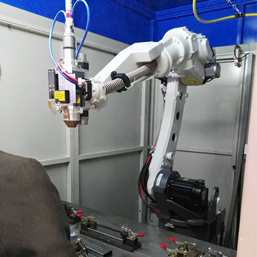
Fiber coupled semiconductor laser systems have higher electro-optic conversion efficiency, more compact volume and more competitive price than fiber lasers. Laser transmission through the fiber output, suitable for use with automation equipment, laser flexible processing.

Sample display
Application industry
Laser welding has been used in microelectronic packaging and assembly, such as reflow welding of high-density lead surface mount devices, reflow welding of heat-sensitive and electrostatic sensitive devices, selective reflow welding, and making of BGA outer lead bumps. Flip chip on-chip convex point fabrication, BGA convex repair, TAB device packaging lead connection, and so on.
  • Name :
  • Compang address :
  • Compang name :
  • Tel :
  • Email :
  • Message :
  • Code :